Startup Originals Team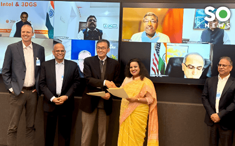
India’s semiconductor ambitions received a major boost after the Odisha government signed a tripartite Memorandum of Understanding (MoU) with Intel and US-based 3D Glass Solutions (3DGS) to establish an advanced glass core substrate manufacturing facility in the state. The project is expected to attract investments of approximately $3.3 billion, making it one of the largest high-technology manufacturing investments announced in India.
The proposed facility will be located in the Bhubaneswar-Khurda region and is expected to play a critical role in strengthening India’s semiconductor supply chain.
A Major Step in India’s Semiconductor Journey
The agreement was signed in the presence of:
- Ashwini Vaishnaw, Union Minister for Electronics and IT
- Mohan Charan Majhi, Chief Minister of Odisha
- Lip-Bu Tan, CEO of Intel
The partnership highlights growing collaboration between global technology leaders and Indian states as the country works to build a domestic semiconductor ecosystem.
What Is a Glass Core Substrate Facility?
Glass core substrates are an advanced component used in semiconductor packaging.
They help:
- Improve chip performance
- Enable higher processing speeds
- Support advanced AI and computing applications
- Increase power efficiency and chip density
As semiconductor technology becomes more sophisticated, advanced packaging solutions are becoming just as important as chip manufacturing itself.
The Odisha facility will focus on producing these next-generation semiconductor packaging materials, which are expected to be critical for future AI, data centre, and high-performance computing technologies.
Why This Project Matters
India currently imports a large share of its semiconductor-related components and technologies.
The proposed facility is expected to:
- Reduce dependence on imports
- Strengthen domestic semiconductor capabilities
- Support electronics manufacturing growth
- Enhance India’s role in global semiconductor supply chains
It also aligns with the Indian government’s broader semiconductor mission aimed at creating a complete chip ecosystem within the country.
Boost for Odisha’s Industrial Ecosystem
The project represents one of the biggest technology investments in Odisha’s history.
Apart from attracting foreign investment, it is expected to:
- Generate high-skilled employment opportunities
- Promote advanced manufacturing capabilities
- Encourage research and innovation ecosystems
- Strengthen the state’s position as an emerging technology hub
The Bhubaneswar-Khurda region is increasingly attracting investments in electronics, manufacturing, and technology sectors.
India’s Push for Semiconductor Self-Reliance
Over the last few years, India has aggressively pursued semiconductor investments through:
- Government incentives
- Production-linked incentive (PLI) schemes
- Global partnerships with technology companies
The country is seeking to become a major player in:
- Semiconductor manufacturing
- Chip packaging
- Electronics production
- AI infrastructure development
Projects involving companies like Intel, Tata Electronics, Micron, and other global players are helping accelerate this vision.
The Bigger Picture
Semiconductors have become a strategic industry worldwide due to their importance in:
- Artificial Intelligence
- Smartphones
- Data centres
- Electric vehicles
- Defence systems
- Industrial automation
As countries compete to secure chip supply chains, investments like the Intel-3DGS-Odisha partnership position India as an emerging destination for advanced semiconductor manufacturing and packaging technologies.
Conclusion
The $3.3 billion semiconductor project in Odisha marks a significant milestone in India’s efforts to build a globally competitive semiconductor ecosystem. With support from Intel and 3D Glass Solutions, the facility could become a key part of India’s strategy to strengthen domestic chip manufacturing, advanced packaging capabilities, and long-term technological self-reliance.