Startup Originals Team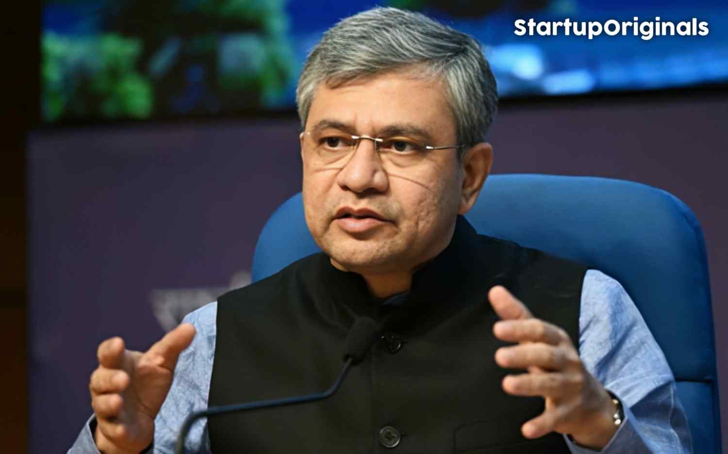
India is making a landmark advance in its electronics sector with the establishment of its first commercial-scale silicon fabrication (fab) facility, featuring a capacity of 50,000 wafer starts per month. This project, announced by Union Minister Ashwini Vaishnaw, puts India on the global semiconductor map and marks a historic leap towards tech self-reliance.
Project Highlights and Scale:
- Location and Investment: The fab is being set up in Dholera, Gujarat, spearheaded by Tata Electronics with Taiwan’s Powerchip Semiconductor Manufacturing Corporation (PSMC), with a massive investment of ₹91,000 crore (about $11 billion).
- Capacity: At full scale, the plant will deliver 50,000 wafer starts per month-surpassing the standard industry range of 20,000–40,000 wafers monthly for such facilities.
- Timeline: Construction is underway and production is expected to begin by late 2026.
Strategic Importance:
- Historic First: Most previous fabs in India, like the SCL in Mohali, have operated only at lab scale. This new project is the country’s first true commercial fab of global significance.
- Ecosystem Development: Along with the fab, India is fast-tracking related infrastructure-Assembly, Testing, Marking, and Packaging (ATMP) units are being set up across the country, with six units in progress and more approvals underway.
- Major Global Partners: Leading equipment makers like Applied Materials and Lam Research are establishing design, production, and real-time validation facilities in India, catalyzing a robust semiconductor ecosystem.
Product Impact and Industry Reach:
- Chip Portfolio: The facility will fabricate power management integrated circuits, display drivers, microcontrollers, and high-performance computing logic chips for sectors such as automotive, AI, telecommunications, and data storage.
- Job Creation: The project is expected to generate over 20,000 direct and indirect skilled jobs, fostering engineering and manufacturing talent domestically.
Policy Support and Leadership:
- Vision and Commitment: Inspired by Prime Minister Narendra Modi’s pledge for “Made in India, Made by Indians” chips before the end of 2025, this initiative is a pillar of India’s mission for technological autonomy and energy transformation.
- Historic Context: While industry pioneers like Robert Noyce sought to set up fabs in India as early as the 1960s, previous attempts were hampered by regulatory hurdles. Today, the government’s mission-driven policy supports a thriving, innovation-driven semiconductor industry.
Conclusion:
The commercial-scale silicon fab in Dholera marks a turning point for India’s semiconductor ambitions, laying the foundation for a self-reliant digital future. With state-of-the-art manufacturing, a growing ecosystem, and strategic investments, India is poised to emerge as a key global player in advanced chip technology.